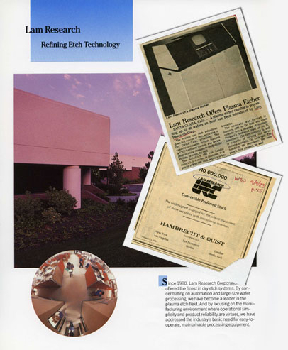

Lam Research’s AutoEtch 480 was a landmark in the history of plasma etchers. ...
A Presentation Draft of The First Wafer Fab Cost Optimization Model1980
Nat was one of the prime movers of EUV and without his perseverance, EUV may ne ...
In 1983 the semiconductor equipment industry was coming out of a two-year slow-d ...
IBM’s EL-1: a milestone in e-beam lithography
When Back End of the Line wafer processing was new and emergent.
One of the most interesting questions to answer is why are Megafabs so popular? ...
All technology revolutions are not so easy. other than in 20:20 hindsight. The i ...
IBM is using 1X x-ray lithography to expose the gate level of 0.15 micron PowerP ...
Silicon mythology has it that node progression is predictable and constant. In r ...
Access to and use of this Website is subject to TechInsights' Terms of Use (including Copyright Policy & Claims) and Privacy Policy. By accessing or using this Website you agree to TechInsights' Terms of Use (including Copyright Policy & Claims) and Privacy Policy.
Copyright © 2025 TechInsights Inc. All rights reserved.